Tormenta Card, Rev. A (S/N 2) 11/18/00,
shown without mounting bracket
Zapata Telephony Tormenta Card, Rev. A 11/8/00

Tormenta Card, Rev. A (S/N 2) 11/18/00,
shown without mounting bracket
NOTE-- MANDITORY Enginerring Change to Rev. A design -- PLEASE READ
Click here if you wish to download the gerber photoplot files for board fabrication
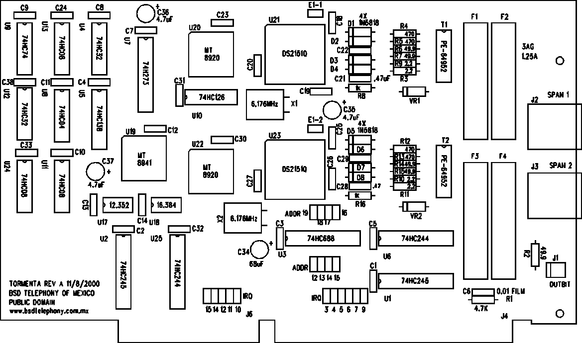
All references to the 74HC688 (U3) is to be understood to really be a reference to a 74HC682 with pin 1 cut off (or lifted). See Enginering Change Notice above.
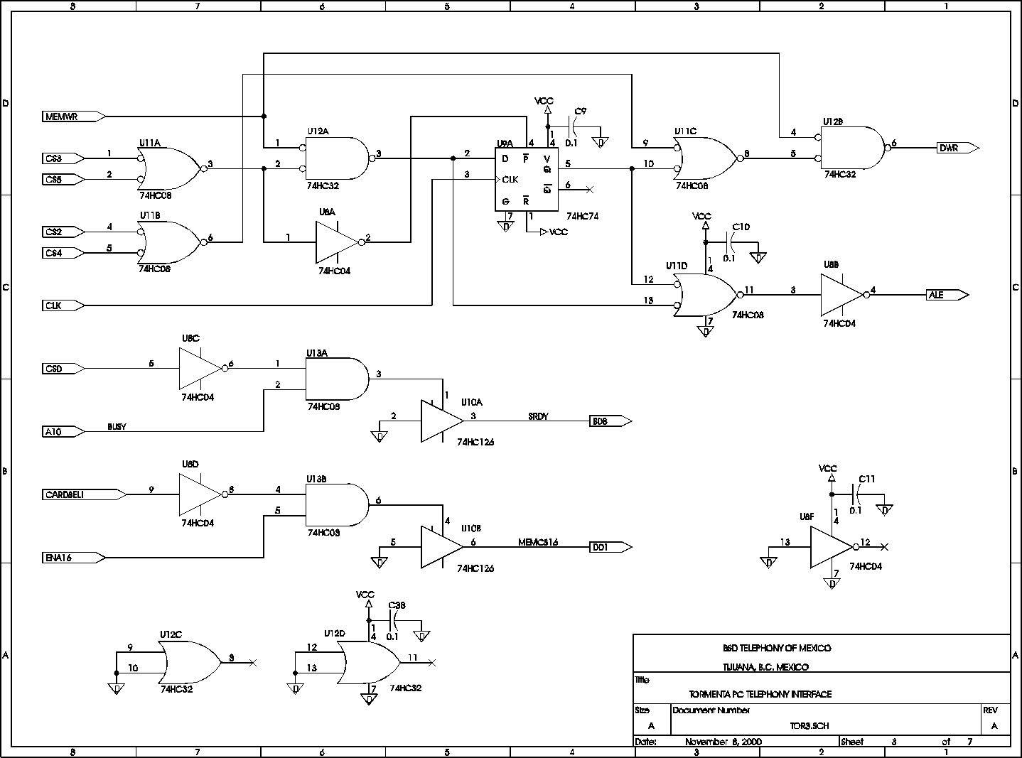
Schematic


Board Artwork
Assembly Drawing

Silk Screen

Note: any traces that appear to be touching each other really aren't. This appearance is a result of (somewhat poor) conversion between the internal CAD system's graphical format and one which could be displayed on the Internet.
Top Layer

Bottom Layer

Solder Mask

Drill Drawing

TORMENTA PC TELEPHONY INTERFACE               Revised:  November  8, 2000
TOR1.SCH                                      Revision: A
Bill Of Materials             November    8, 2000     16:23:28     Page    1
 Item  Quantity  Reference                 Part
__________________________________________________________
    1      28    C1,C2,C3,C4,C5,C7,C8,C9,  0.1    Ceramic
                 C10,C11,C12,C13,C14,C18,
                 C19,C20,C22,C23,C24,C25,
                 C26,C27,C29,C30,C31,C32,
                 C33,C38
2 1 C6 0.01 Film
3 2 C21,C28 0.47 Ceramic
4 1 C34 68uF 10 Volt Tantalum
5 3 C35,C36,C37 4.7uF 10 Volt Tantalum
6 8 D1,D2,D3,D4,D5,D6,D7,D8 1N5818
7 4 F1,F2,F3,F4 FUSE 3AG 1.25 AMP
    8       8    JP1,JP2,JP3,JP4,JP5,JP6,  JUMPER
                 JP7,JP8
9 1 JP9 JUMPER E1-1
10 1 JP10 JUMPER E1-2
11 1 JP11 JUMPER IRQ3
12 1 JP12 JUMPER IRQ4
13 1 JP13 JUMPER IRQ5
14 1 JP14 JUMPER IRQ6
15 1 JP15 JUMPER IRQ7
16 1 JP16 JUMPER IRQ9
17 1 JP17 JUMPER IRQ10
18 1 JP18 JUMPER IRQ11
19 1 JP19 JUMPER IRQ12
20 1 JP20 JUMPER IRQ14
21 1 JP21 JUMPER IRQ15
22 1 J1 OUTBIT CONNECTOR
23 2 J2,J3 8 PIN MODULAR JACK
24 1 J4 ISA BUS, A CONNECTOR
TORMENTA PC TELEPHONY INTERFACE               Revised:  November  8, 2000
TOR1.SCH                                      Revision: A
Bill Of Materials             November    8, 2000     16:23:28     Page    2
 Item  Quantity  Reference                 Part
__________________________________________________________
25 1 J5 ISA BUS, B CONNECTOR
26 1 J6 ISA BUS, C CONNECTOR
27 1 J7 ISA BUS, D CONNECTOR
28 1 R1 4.7K 5% 1/4 W
29 5 R2,R6,R7,R14,R15 49.9 1% 1/4 W
30 4 R3,R9,R10,R11 2.2 5% 1/4 W
31 4 R4,R5,R12,R13 470 1% 1/4 W
32 2 R8,R16 1K 5% 1/4 W
33 2 T1,T2 XFMR PULSE PE-64952
34 2 U1,U2 74HC245
35 1 U3 74HC682, w/Pin 1 cut (or lifted)
36 2 U4,U12 74HC32
37 1 U5 74HC138
38 2 U6,U25 74HC244
39 1 U7 74HC273
40 1 U8 74HC04
41 1 U9 74HC74
42 1 U10 74HC126
43 3 U11,U13,U24 74HC08
44 1 U17 OSC 12.352MHz
45 1 U18 OSC 16.384MHz
46 1 U19 MT8941PLCC
47 2 U20,U22 MT8920PLCC
48 2 U21,U23 DS2151QB
49 2 VR1,VR2 TRANZORB BI 25V
50 2 X1,X2 CRYSTAL 6.176MHz
With the exception of items protected by the GNU General Public License (which are
clearly indicated as such), the technologies, software, hardware, designs, drawings,
schematics, board layouts and/or artwork, concepts, methodologies (including the use of
all of these, and that which is derived from the use of all of these), all other
intellectual properties contained herein, and all intellectual property rights have been
and shall continue to be expressly for the benefit of all mankind, and are perpetually
placed in the public domain, and may be used, copied, and/or modified by anyone, in any
manner, for any legal purpose, without restriction.